Buttons and test jig (2/7/20)
Printing our own buttons
Our first volume batch of PCBAs (Printed Circuit Board Assemblies) should be coming any day. The software is in good enough shape to ship but we need to get ready to assemble boards when they arrive. We already have more than enough enclosures for the boards, but we need to be ready with a batch of buttons for them and to be able to quickly program and test the boards. We decided to purchase a used Form 2 Selective Laster Sintering (SLS) resin printer to help with the process. With Signet we had the buttons resin printed through a service and now we are printing them ourselves.
You can see the first batch of printed buttons below:
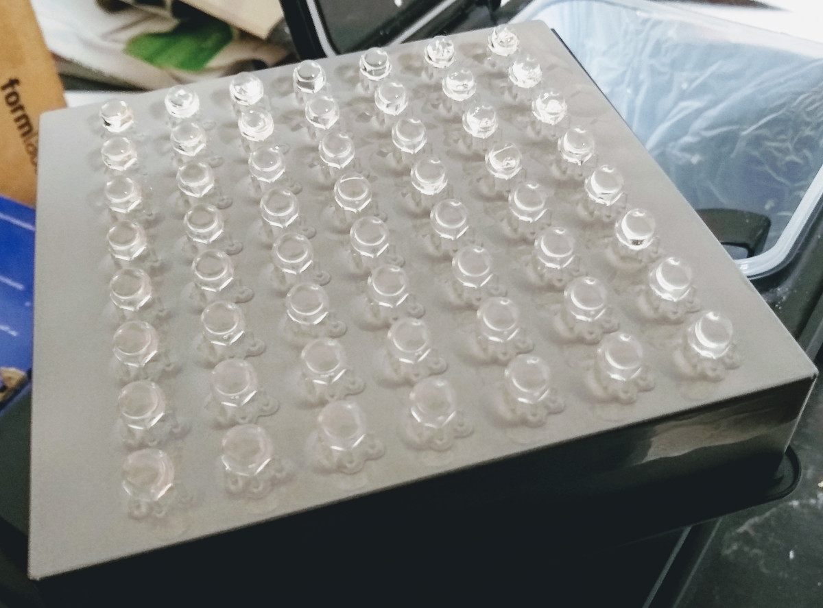
SLS printers are much more precise than Fused Deposition Modeling (FDM) printers, but we still need to allow for a certain amount of variability due to resin curing in the wrong places and shrinking and warping during curing. By doing the printing ourselves we could quickly do iterations to design around these variables to get a better fit in the enclosure: Not so loose that the button rattles in the enclosure and not so tight that it binds.
Building the test jig
With Signet we were able to program the units by using the USB-based Device Firmware Update (DFU) bootloader already built into the microcontroller. This meant that we didn’t need to make any internal electrical connections to program the boards. With Signet HC, the DFU bootloader does not run over the high-speed USB port so we need to make temporary electrical connections to the board to program it. We decided we would program the device over the Serial Wire Debug (SWD) port using a custom test jig. Since there are no connectors installed on the board the best solution is for us is was to create a “bed of nails” test jig, whereby spring-loaded pogo pins are mounted to a platform and the board rests on the pins. A separate tool presses the board onto the pins to make a solid connection. We modeled our jig in FreeCad and printed it on our Form2 printer. You can see the CAD model below:
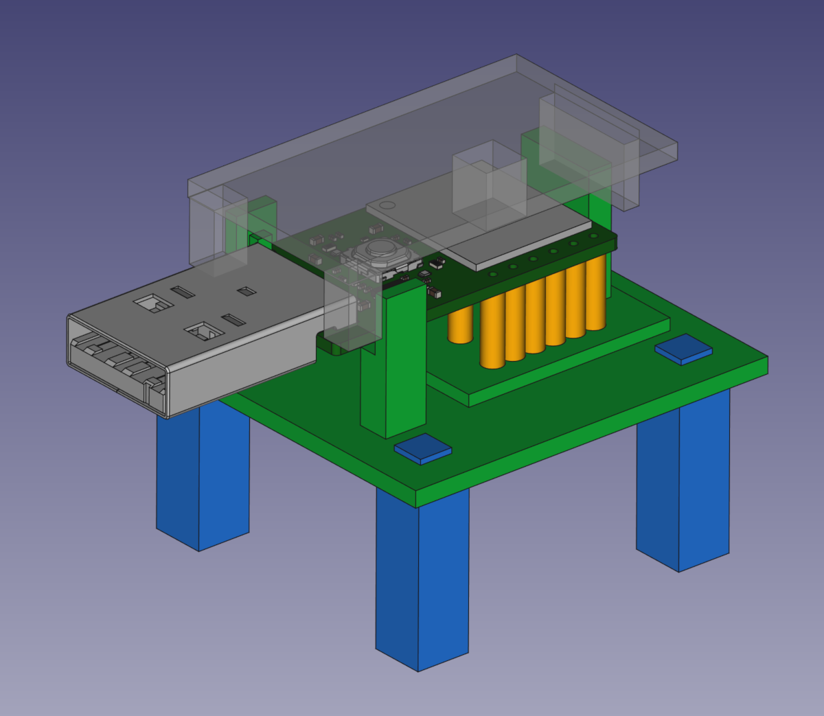
The light green area is the pin platform. In addition to holes to mount the pogo pins and legs it has three supports to both hold the board in position and level the board when it’s pushed down. The gray transparent part pushes down on the top of the eMMC chip and around the USB port and slots closely over the board supports making it easy to get into position. You can see the final printed jig below:
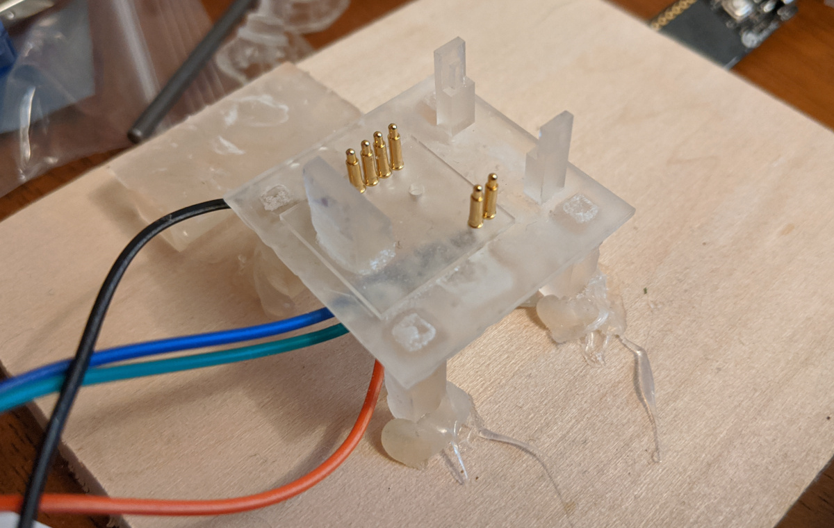
To finish the assembly we added a little super glue to the platform legs and hot glued them to a wood platform. It’s crude but effective. You can see below how everything fits together when in use.
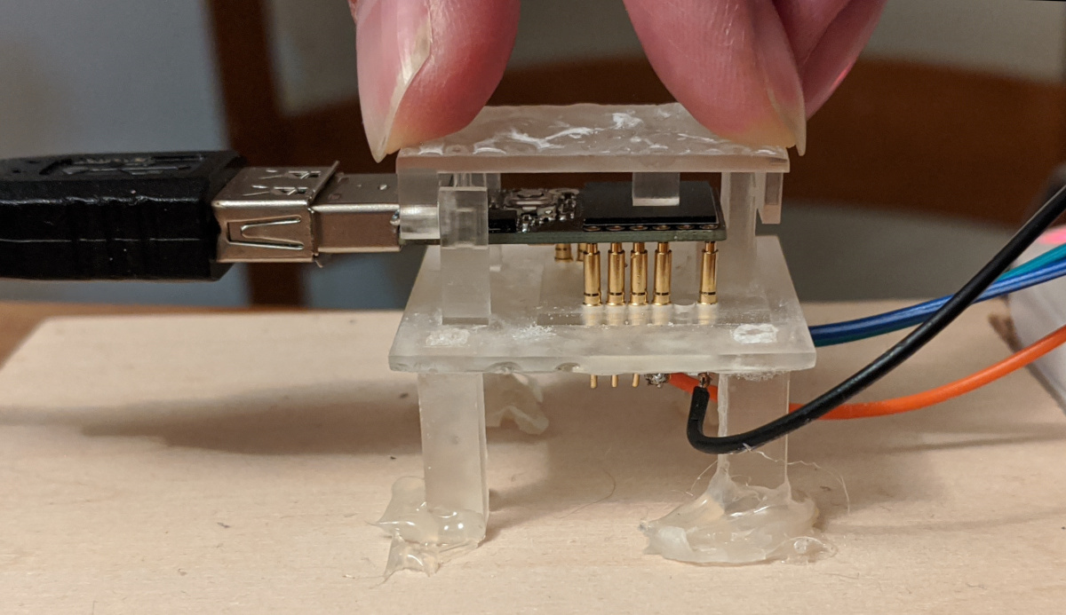
Our testing jig could be considered an internal process not worthy of external documentation, but this is the first time we’ve ever made one and we found somewhat limited information about how to make these sorts of jigs in our research. We hope that the sharing of it helps others.